Unit-cell in HFSS
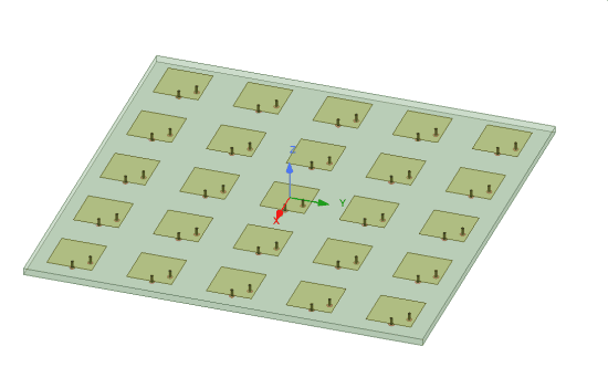
HFSS offers different method of creating and simulating a large array. The explicit method, shown in Figure 1(a) might be the first method that comes to our mind. This is where you create the exact CAD of the array and solve it. While this is the most accurate method of simulating an array, it is computationally extensive. This method may be non-feasible for the initial design of a large array. The use of unit cell (Figure 1(b)) and array theory helps us to start with an estimate of the array performance by a few assumptions. Finite Array Domain Decomposition (or FADDM) takes advantage of unit cell simplicity and creates a full model using the meshing information generated in a unit cell. In this blog we will review the creation of unit cell. In the next blog we will explain how a unit cell can be used to simulate a large array and FADDM.


In a unit cell, the following assumptions are made:
- The pattern of each element is identical.
- The array is uniformly excited in amplitude, but not necessarily in phase.
- Edge affects and mutual coupling are ignored

A unit cell works based on Master/Slave (or Primary/Secondary) boundary around the cell. Master/Slave boundaries are always paired. In a rectangular cell you may use the new Lattice Pair boundary that is introduced in Ansys HFSS 2020R1. These boundaries are means of simulating an infinite array and estimating the performance of a relatively large arrays. The use of unit cell reduces the required RAM and solve time.
Primary/Secondary (Master/Slave) (or P/S) boundaries can be combined with Floquet port, radiation or PML boundary to be used in an infinite array or large array setting, as shown in Figure 3.

To create a unit cell with P/S boundary, first start with a single element with the exact dimensions of the cell. The next step is creating a vacuum or airbox around the cell. For this step, set the padding in the location of P/S boundary to zero. For example, Figure 4 shows a microstrip patch antenna that we intend to create a 2D array based on this model. The array is placed on the XY plane. An air box is created around the unit cell with zero padding in X and Y directions.


You notice that in this example the vacuum box is larger than usual size of quarter wavelength that is usually used in creating a vacuum region around the antenna. We will get to calculation of this size in a bit, for now let’s just assign a value or parameter to it, as it will be determined later. The next step is to define P/S to generate the lattice. In AEDT 2020R1 this boundary is under “Coupled” boundary. There are two methods to create P/S: (1) Lattice Pair, (2) Primary/Secondary boundary.
Lattice Pair
The Lattice Pair works best for square lattices. It automatically assigns the primary and secondary boundaries. To assign a lattice pair boundary select the two sides that are supposed to create infinite periodic cells, right-click->Assign Boundary->Coupled->Lattice Pair, choose a name and enter the scan angles. Note that scan angles can be assigned as parameters. This feature that is introduced in 2020R1 does not require the user to define the UV directions, they are automatically assigned.


Primary/Secondary
Primary/Secondary boundary is the same as what used to be called Master/Slave boundary. In this case, each Secondary (Slave) boundary should be assigned following a Primary (Master) boundary UV directions. First choose the side of the cell that Primary boundary. Right-click->Assign Boundary->Coupled->Primary. In Primary Boundary window define U vector. Next select the secondary wall, right-click->Assign Boundary->Couple->Secondary, choose the Primary Boundary and define U vector exactly in the same direction as the Primary, add the scan angles (the same as Primary scan angles)

Floquet Port and Modes Calculator
Floquet port excites and terminates waves propagating down the unit cell. They are similar to waveguide modes. Floquet port is always linked to P/S boundaries. Set of TE and TM modes travel inside the cell. However, keep in mind that the number of modes that are absorbed by the Floquet port are determined by the user. All the other modes are short-circuited back into the model. To assign a Floquet port two major steps should be taken:
Defining Floquet Port
Select the face of the cell that you like to assign the Floquet port. This is determined by the location of P/S boundary. The lattice vectors A and B directions are defined by the direction of lattice (Figure 7).

The number of modes to be included are defined with the help of Modes Calculator. In the Mode Setup tab of the Floquet Port window, choose a high number of modes (e.g. 20) and click on Modes Calculator. The Mode Table Calculator will request your input of Frequency and Scan Angles. After selecting those, a table of modes and their attenuation using dB/length units are created. This is your guide in selecting the height of the unit cell and vaccume box. The attenation multiplied by the height of the unit cell (in the project units, defined in Modeler->Units) should be large enough to make sure the modes are attenuated enough so removing them from the calcuatlion does not cause errors. If the unit cell is too short, then you will see many modes are not attenuated enough. The product of the attenuatin and height of the airbox should be at least 50 dB. After the correct size for the airbox is calcualted and entered, the model with high attenuation can be removed from the Floquet port definition.
The 3D Refinement tab is used to control the inclusion of the modes in the 3D refinement of the mesh. It is recommended not to select them for the antenna arrays.

In our example, Figure 8 shows that the 5th mode has an attenuation of 2.59dB/length. The height of the airbox is around 19.5mm, providing 19.5mm*2.59dB/mm=50.505dB attenuation for the 5th mode. Therefore, only the first 4 modes are kept for the calculations. If the height of the airbox was less than 19.5mm, we would need to increase the height so accordingly for an attenuation of at least 50dB.
Radiation Boundary
A simpler alternative for Floquet port is radiation boundary. It is important to note that the size of the airbox should still be kept around the same size that was calculated for the Floquet port, therefore, higher order modes sufficiently attenuated. In this case the traditional quarter wavelength padding might not be adequate.

Perfectly Matched Layer
Although using radiation boundary is much simpler than Floquet port, it is not accurate for large scan angles. It can be a good alternative to Floquet port only if the beam scanning is limited to small angles. Another alternative to Floquet port is to cover the cell by a layer of PML. This is a good compromise and provides very similar results to Floquet port models. However, the P/S boundary need to surround the PML layer as well, which means a few additional steps are required. Here is how you can do it:
- Reduce the size of the airbox* slightly, so after adding the PML layer, the unit cell height is the same as the one that was generated using the Modes Calculation. (For example, in our model airbox height was 19mm+substrte thickness, the PML height was 3mm, so we reduced the airbox height to 16mm).
- Choose the top face and add PML boundary.
- Select each side of the airbox and create an object from that face (Figure 10).
- Select each side of the PML and create objects from those faces (Figure 10).
- Select the two faces that are on the same plane from the faces created from airbox and PML and unite them to create a side wall (Figure 10).
- Then assign P/S boundary to each pair of walls (Figure 10).
*Please note for this method, an auto-size “region” cannot be used, instead draw a box for air/vacuum box. The region does not let you create the faces you need to combine with PML faces.

The advantage of PML termination over Floquet port is that it is simpler and sometimes faster calculation. The advantage over Radiation Boundary termination is that it provides accurate results for large scan angles. For better accuracy the mesh for the PML region can be defined as length based.
Seed the Mesh
To improve the accuracy of the PML model further, an option is to use length-based mesh. To do this select the PML box, from the project tree in Project Manager window right-click on Mesh->Assign Mesh Operation->On Selection->Length Based. Select a length smaller than lambda/10.

Scanning the Angle
In phased array simulation, we are mostly interested in the performance of the unit cell and array at different scan angles. To add the scanning option, the phase of P/S boundary should be defined by project or design parameters. The parameters can be used to run a parametric sweep, like the one shown in Figure 12. In this example the theta angle is scanned from 0 to 60 degrees.

Comparing PML and Floquet Port with Radiation Boundary
To see the accuracy of the radiation boundary vs. PML and Floquet Port, I ran the simulations for scan angles up to 60 degrees for a single element patch antenna. Figure 13 shows that the accuracy of the Radiation boundary drops after around 15 degrees scanning. However, PML and Floquet port show similar performance.


S Parameters
To compare the accuracy, we can also check the S parameters. Figure 14 shows the comparison of active S at port 1 for PML and Floquet port models. Active S parameters were used since the unit cell antenna has two ports. Figure 15 shows how S parameters compare for the model with the radiation boundary and the one with the Floquet port.


Conclusion
The unit cell definition and options on terminating the cell were discussed here. Stay tuned. In the next blog we discuss how the unit cell is utilized in modeling antenna arrays.