
In this article I will cover a Voltage Drop (DC IR) simulation in SIwave, applying realistic power delivery setup on a simple 4-layer PCB design. The main goal for this project is to understand what data we receive by running DC IR simulation, how to verify it, and what is the best way of using it.
And before I open my tools and start diving deep into this topic, I would like to thank Zachary Donathan for asking the right questions and having deep meaningful technical discussions with me on some related subjects. He may not have known, but he was helping me to shape up this article in my head!
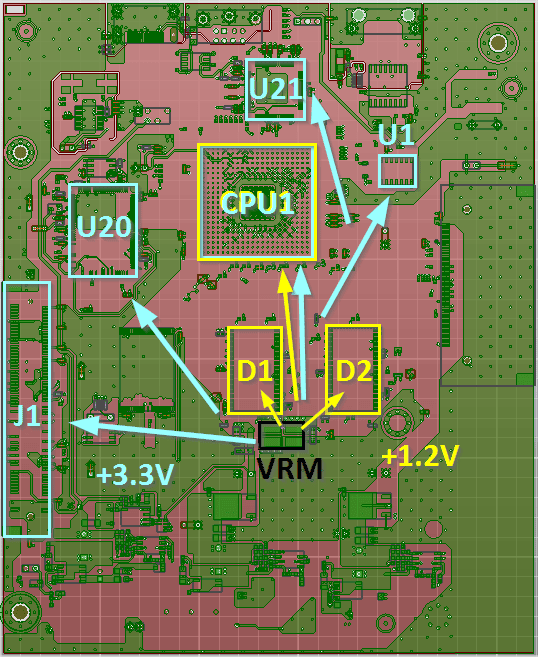
Design Setup
There are many different power nets present on the board under test, however I will be focusing on two widely spread nets +1.2V and +3.3V. Both nets are being supplied through Voltage Regulator Module (VRM), which will be assigned as a Voltage Source in our analysis. After careful assessment of the board design, I identified the most critical components for the power delivery to include in the analysis as Current Sources (also known as ‘sinks’). Two DRAM small outline integrated circuit (SOIC) components D1 and D2 are supplied with +1.2V. While power net +3.3V provides voltage to two quad flat package (QFP) microcontrollers U20 and U21, mini PCIE connector, and hex Schmitt-Trigger inverter U1.

Figure 1 shows the ‘floor plan’ of the DC IR analysis setup with 1.2V voltage path highlighted in yellow and 3.3V path highlighted in light blue.
Before we assign any Voltage and Current sources, we need to define pin groups for all nets +1.2V, +3.3V and GND for all PDN component mentioned above. Having pin groups will significantly simplify the reviewing process of the results. Also, it is generally a good practice to start the DC IR analysis from the ‘big picture’ to understand if certain component gets enough power from the VRM. If a given IC reports an acceptable level of voltage being delivered with a good margin, then we don’t need to dig deeper; we can instead focus on those which may not have good enough margins.
Once we have created all necessary pin groups, we can assign voltage and current sources. There are several ways of doing that (using wizard or manual), for this project we will use ‘Generate Circuit Element on Components’ feature to manually define all sources. Knowing all the components and having pin groups already created makes the assignment very straight-forward. All current sources draw different amount of current, as indicated in our setting, however all current sources have the same Parasitic Resistance (very large value) and all voltage source also have the same Parasitic Resistance (very small value). This is shown on Figure 2 and Figure 3.
Note: The type of the current source ‘Constant Voltage’ or ‘Distributed Current’ matters only if you are assigning a current source to a component with multiple pins on the same net, and since in this project we are working with pins groups, this setting doesn’t make difference in final results.


For each power net we have created a voltage source on VRM and multiple current sources on ICs and the connector. All sources have a negative node on a GND net, so we have a good common return path. And in addition, we have assigned a negative node of both voltage sources (one for +1.2V and one for +3.3V) as our reference points for our analysis. So reported voltage values will be referenced to that that node as absolute 0V.
At this point, the DC IR setup is complete and ready for simulation.
Results overview and validation
When the DC IR simulation is finished, there is large amount of data being generated, therefore there are different ways of viewing results, all options are presented on Figure 4. In this article I will be primarily focusing on ‘Power Tree’ and ‘Element Data’. As an additional source if validation we may review the currents and voltages overlaying the design to help us to visualize the current flow and power distribution. Most of the time this helps to understand if our assumption of pin grouping is accurate.

Power Tree
First let’s look at the Power Tree, presented on Figure 5. Two different power nets were simulated, +1.2V and +3.3V, each of which has specified Current Sources where the power gets delivered. Therefore, when we analyze DC IR results in the Power tree format, we see two ‘trees’, one for each power net. Since we don’t have any pins, which would get both 1.2V and 3.3V at the same time (not very physical example), we don’t have ‘common branches’ on these two ‘trees’.
Now, let’s dissect all the information present in this power tree (taking in consideration only one ‘branch’ for simplicity, although the logic is applicable for all ‘branches’):
- We were treating both power nets +1.2V and +3.3V as separate voltage loops, so we have assigned negative nodes of each Voltage Source as a reference point. Therefore, we see the ‘GND’ symbol ((1) and (2)) for each voltage source. Now all voltage calculations will be referenced to that node as 0V for its specific tree.
- Then we see the path from Voltage Source to Current Source, the value ΔV shows the Voltage Drop in that path (3). Ultimately, this is the main value power engineers usually are interested in during this type of analysis. If we subtract ΔV from Vout we will get the ‘Actual Voltage’ delivered to the specific current source positive pin (1.2V – 0.22246V = 0.977V). That value reported in the box for the Current Source (4). Technically, the same voltage drop value is reported in the column ‘IR Drop’, but in this column we get more details – we see what the percentage of the Vout is being dropped. Engineers usually specify the margin value of the acceptable voltage drop as a percentage of Vout, and in our experiment we have specified 15%, as reported in column ‘Specification’. And we see that 18.5% is greater than 15%, therefore we get ‘Fail_I_&_V’ results (6) for that Current Source.
- Regarding the current – we have manually specified the current value for each Current Source. Current values in Figure 2 are the same as in Figure 5. Also, we can specify the margin for the current to report pass or fail. In our example we assigned 108A as a current at the Current Source (5), while 100A is our current limit (4). Therefore, we also got failed results for the current as well.
- As mentioned earlier, we assigned current values for each Current Source, but we didn’t set any current values for the Voltage Source. This is because the tool calculates how much current needs to be assigned for the Voltage Source, based on the value at the Current Sources. In our case we have 3 Current Sources 108A, 63A, 63A (5). The sum of these three values is 234A, which is reported as a current at the Voltage Source (7). Later we will see that this value is being used to calculate output power at the Voltage Source.

Element Data
This option shows us results in the tabular representation. It lists many important calculated data points for specific objects, such as bondwire, current sources, all vias associated with the power distribution network, voltage probes, voltage sources.
Let’s continue reviewing the same power net +1.2V and the power distribution to CPU1 component as we have done for Power Tree (Figure 5). The same way we will be going over the details in point-by-point approach:
- First and foremost, when we look at the information for Current Sources, we see a ‘Voltage’ value, which may be confusing. The value reported in this table is 0.7247V (8), which is different from the reported value of 0.977V in Power Tree on Figure 5 (4). The reason for the difference is that reported voltage value were calculated at different locations. As mentioned earlier, the reported voltage in the Power Tree is the voltage at the positive pin of the Current Source. The voltage reported in Element Data is the voltage at the negative pin of the Current Source, which doesn’t include the voltage drop across the ground plane of the return path.
To verify the reported voltage values, we can place Voltage Probes (under circuit elements). Once we do that, we will need to rerun the simulation in order to get the results for the probes:
- Two terminals of the ‘VPROBE_1’ attached at the positive pin of Voltage Source and at the positive pin of the Current Source. This probe should show us the voltage difference between VRM and IC, which also the same as reported Voltage Drop ΔV. And as we can see ‘VPROBE_1’ = 222.4637mV (13), when ΔV = 222.464mV (3). Correlated perfectly!
- Two terminals of the ‘VPROBE_GND’ attached to the negative pin of the Current Source and negative pin of the Voltage Source. The voltage shown by this probe is the voltage drop across the ground plane.
If we have 1.2V at the positive pin of VRM, then voltage drops 222.464mV across the power plane, so the positive pin of IC gets supplied with 0.977V. Then the voltage at the Current Source 0.724827V (8) being drawn, leaving us with (1.2V – 0.222464V – 0.724827V) = 0.252709V at the negative pin of the Current Source. On the return path the voltage drops again across the ground plane 252.4749mV (14) delivering back at the negative pin of VRM (0.252709V – 0.252475V) = 234uV. This is the internal voltage drop in the Voltage Source, as calculated as output current at VRM 234A (7) multiplied by Parasitic Resistance 1E-6Ohm (Figure 3) at VRM. This is Series R Voltage (11)
- Parallel R Current of the Current source is calculated as Voltage 724.82mV (8) divided by Parasitic Resistance of the Current Source (Figure 3) 5E+7 Ohm = 1.44965E-8 (9)
- Current of the Voltage Source report in the Element Data 234A (10) is the same value as reported in the Power Tree (sum of all currents of Current Sources for the +1.2V power net) = 234A (7). Knowing this value of the current we can multiple it by Parasitic Resistance of the Voltage Source (Figure 3) 1E-6 Ohm = (234A * 1E-6Ohm) = 234E-6V, which is equal to reported Series R Voltage (11). And considering that the 234A is the output current of the Voltage Source, we can multiple it by output voltage Vout = 1.2V to get a Power Output = (234A * 1.2V) = 280.85W (12)

In addition to all provided above calculations and explanations, the video below in Figure 7 highlights all the key points of this article.
Conclusion
By carefully reviewing the Power Tree and Element Data reporting options, we can determine many important decisions about the power delivery network quality, such as how much voltage gets delivered to the Current Source; how much voltage drop is on the power net and on the ground net, etc. More valuable information can be extracted from other DC IR results options, such as ‘Loop Resistance’, ‘Path Resistance’, ‘RL table’, ‘Spice Netlist’, full ‘Report’. However, all these features deserve a separate topic.
As always, if you would like to receive more information related to this topic or have any questions please reach out to us at info@padtinc.com.