Simulation itself is no longer a new concept in engineering, but individual fields, applications, and physics are continually improved upon and integrated into the toolbox that is an engineer’s arsenal. Many times, these are incremental additions to a particular solver’s capabilities or a more specialized method of post processing, however this can also occasionally be present through new cross-connections between separate tools or even an entirely new piece of software. As a result of all this, Ansys has now reached critical mass for its solution space surrounding Electronics Reliability. That is, we can essentially approach an electronics reliability problem from any major physics perspective that we like.
So, what is Electronics Reliability and what physics am I referring to? Great question, and I’m glad you asked – I’d like to run through some examples of each physics and their typical use-case / importance, as well as where Ansys fits in. Of course, real life is a convoluted Multiphysics problem in most cases, so having the capability to accommodate and link many different physics together is also an important piece of this puzzle.
Running down the list, we should perhaps start with the most obvious category given the name – Electrical Reliability. In a broad sense, this encompasses all things related to electromagnetic fields as they pertain to transmission of both power and signals. While the electrical side of this topic is not typically in my wheelhouse, it is relatively straightforward to understand the basics around a couple key concepts, Power Integrity and Signal Integrity.
Power integrity, as its name suggests, is the idea that we need to maintain certain standards of quality for the electrical power in a device/board/system. While some kinds of electronics are robust enough that they will continue to function even under large variations in supplied voltage or current, there are also many that rely on extremely regular power supplies that only vary above certain limits or within narrow bounds. Even if we’re looking at a single PCB (as in the image below), in today’s technological environment it will no doubt have electrical traces mapped all throughout it as well as multiple devices present that operate under their own specified electrical conditions.

If we were determined to do so, we could certainly measure trace lengths, widths, thicknesses, etc., and make some educated guesses for the resulting voltage drops to individual components. However, considerably more effort would need to be made to account for bends, corners, or variable widths, and that would still completely neglect any environmental effects or potential interactions between traces. It is much better to be able to represent and solve for the entire geometry at once using a dedicated field solver – this is where Ansys SIwave or Ansys HFSS typically come in, giving us the flexibility to accurately determine the electrical reliability, whether we’re talking about AC or DC power sources.
Signal integrity is very much related, except that “signals” in this context often involve different pathways, less energy, and a different set of regulations and tolerances. Common applications involve Chip-signal modeling and DDRx virtual compliance – these have to do with not only the previous general concerns regarding stability and reliability, but also adherence to specific standards (JEDEC) through virtual compliance tests. After all, inductive electromagnetic effects can still occur over nonconductive gaps, and this can be a significant source of noise and instability in cases where conductive paths (like board traces or external connections) cross or run very near each other.

Whether we are looking at timings between components, transition times, jitter, or even just noise, HFSS and SIWave can both play roles here. In either case, being able to use a simulation environment to confirm that a certain design will or will not meet certain standards can provide invaluable feedback to the design process.
Other relevant topics to Electrical Reliability may include Electromagnetic Interference (EMI) analysis, antenna performance, and Electrostatic Discharge (ESD) analysis. While I will not expand on these in great detail here, I think it is enough to realize that an excellent electrical design (such as for an antenna) requires some awareness of the operational environment. For instance, we might want to ensure that our chosen or designed component will adequately function while in the presence of some radiation environment, or maybe we would like to test the effectiveness of the environmental shielding on a region of our board. Maybe, there is some concern about the propagation of an ESD through a PCB, and we would like to see how vulnerable certain components are. Ansys tools provide us the capabilities needed to do all of this.
The second area of primary interest is Thermal Reliability, as just about anyone who has worked with or even used electronics knows, they generate some amount of heat while in use. Of course, the quantity, density, and distribution of that heat can vary tremendously depending on the exact device or system under question, but this heat will ultimately result in a rise in temperature somewhere. The point of thermal reliability basically boils down to realizing that the performance and function of many electrical components depends on their temperature. Whether it is simply a matter of accounting for a change in electrical conductivity as temperature rises or a hard limit of functionality for a particular transistor at 150 °C, acknowledging and accounting for these thermal effects is critical when considering electronics reliability. This is a problem with several potential solutions depending on the scale of interest, but generally we cover the package/chip, board, and full system levels. For the component/chip level, a designer will often want to provide some package level specs for OEMs so that a component can be properly scoped in a larger design. Ansys Icepak has toolkits available to help with this process; whether it is simplifying a 3D package down to a detailed network thermal model or identifying the most critical hot spot within a package based on a particular heat distribution. Typically, network models are generated through temperature measurements taken from a sample in a standardized JEDEC test chamber, but Icepak can assist through automatically generating these test environments, as below, and then using simulation results to extract well defined JB and JC values for the package under test.

On the PCB level of detail, we are likely interested in how heat moves across the entire board from component to component or out to the environment. Ansys Icepak lets us read in a detailed ECAD description for said PCB and process its trace and via definitions into an accurate thermal conductivity map that will improve our simulation accuracy. After all, two boards with identical sizing and different copper trace layouts may conduct heat very differently from each other.

On the system level of thermal reliability, we are likely looking at the effectiveness of a particular cooling solution on our electronic design. Icepak makes it easy to include the effects of a heat exchanger (like a coldplate) without having to explicitly model its computationally expensive geometry by using a flow network model. Also, many of today’s electronics are expected to constantly run right up against their limit and are kept within thermal spec by using software to throttle their input power in conjunction with an existing cooling strategy. We can use Icepak to implement and test these dynamic thermal management algorithms so that we can track and evaluate their performance across a range of environmental conditions.
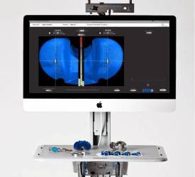
The next topic that we should consider is that of Mechanical Reliability. Mechanical concepts tend to be a little more intuitive and relatable due to their more hands-on nature than the other two, though the exact details behind the cause and significance of stresses in materials is of course more involved. In the most general sense, stress is a result of applying force to an object. If this stress is high compared to what is allowed by a material, then bad things tend to happen – like permanent deformation or fracture. For electronic devices consisting of many materials, small structures, and particularly delicate components, we have once again surpassed what can be reasonably accomplished with hand calculations. Whether we are looking at an individual package, the integrity of an entire PCB, or the stability that a rigid housing will provide to a set of PCBs, Ansys has a solution. We might use Ansys Mechanical to look at manufacturing allowances for the permissible force used while mounting a complicated leaded component onto a board, as seen below. Or maybe, we will use mechanical simulation to find the optimal positioning of leads on a new package such that its natural vibrational frequencies are outside normal ambient conditions.

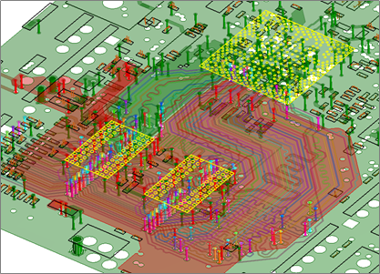
At the PCB level, we face many of the same detail-oriented challenges around representing traces and vias that have been mentioned for the electrical applications. They may not be quite as critical and more easily approximated in some ways, but that does not change the fact that copper traces are mechanically quite different from the resin composites often used as the substrate (like FR-4). Ansys tools like Sherlock provide best in class PCB modeling on this front, allowing us to directly bring in ECAD models with full trace and component detail, and then model them mechanically at several different levels depending on the exact need. Automating a materials property averaging scheme based on the local density of traces may be sufficient if we are looking at the general bending behavior of a board, but we can take it to the next level by explicitly modeling traces as “reinforcement” elements. This brings us to the level of detail where we can much more reliably look at the stresses present in individual traces, such that we can make good design decisions to reduce the risk of traces peeling or delaminating from the surface.

Beyond just looking at possible improvements in the design process, we can also make use of Ansys tools like LS-DYNA or Mechanical to replicate testing or accident conditions that an existing design could be subjected to. As a real-world example, many of us are all too familiar with the occasional consequences of accidentally dropping our smart phones – Ansys is used to test designs against these kind of shock events, where impact against a hard surface can result in high stresses in key locations. This helps us understand where to reinforce a design to protect against the worst damage or even what angle of impact is most likely to cause an operational failure.
As the finale for all of this, I come back to the first comment of reality being a complex Multiphysics problem. Many of the previous topics are not truly isolated to their respective physics (as much as we often simplify them as such), and this is one of the big ways in which the Ansys ecosystem shines: Comprehensive Multiphysics. For the topic of thermal reliability, I simply stated that electronics give off heat. This may be obvious, but that heat is not just a magical result of the device being turned on but is instead a physical and calculable result of the actual electrical behavior. Indeed, this the exact kind of result that we can extract from one of the relevant electronics tools. An HFSS solution will provide us with not only the electrical performance of an antenna but also the three-dimensional distribution of heat that is consequently produced. Ansys lets us very easily feed this information into an Icepak simulation, which then has the ability to give us far more accurate results than a typical uniform heat load assumption provides.

If we find that our temperatures are particularly high, we might then decide to bring these results back into HFSS to locally change material properties as a function of temperature to get an even more accurate set of electrical results. It could be that this results in an appreciable shift in our antenna’s frequency, or perhaps the efficiency has decreased, and aspects of the design need to be revisited. These are some of the things that we would likely miss without a comprehensive Multiphysics environment.
On a more mechanical side, the effects on stress and strain from thermal conditions are very well known and understood at this point, but there is no reason we could not use Ansys to bring the electrical alongside this established thermal-mechanical behavior. After all, what is a better representation of the real physics involved than using SIwave or HFSS to model the electrical behavior of a PCB, bringing those result into an Icepak simulation as a heat load to test the performance of a cooling loop or heat sink, and then using at least some of those thermal results to look at stresses through not only a PCB as a whole but also individual traces? Not a whole lot at this moment in time, I would say.
The extension that we can make on these examples, is that they have by and large been representative cases of how an electronics device responds to a particular event or condition and judging its reliability metrics based on that set of results, however many physics might be involved. There is one more piece of the puzzle we have access to that also interweaves itself throughout the Multiphysics domain and that is Reliability Physics. This is mostly relevant to us in electronics reliability for considering how different events, or even just a repetition of the same event, can stack together and accumulate to contribute towards some failure in the future. An easy example of this is a plastic hinge or clip that you might find on any number of inexpensive products – flexing a thin piece of plastic like in these hinges can provide a very convenient method of motion for quite some time, but that hinge will gradually accumulate damage until it inevitably cracks and fails. Every connection within a PCB is susceptible to this same kind of behavior, whether it is the laminations of the PCB itself, the components soldered to the surface, or even the individual leads on a component. If our PCB is mounted on the control board of a bus, satellite, or boat, there will be some vibrations and thermal cycles associated with its life. A single one of these events may be of much smaller magnitude and seemingly negligible compared to something dramatic like a drop test, and yet they can still add up to the point of being significant over a period of months or years.
This is exactly the kind of thing that Ansys Sherlock proves invaluable for: letting us define and track the effect of events that may occur over a PCB’s entire lifecycle. Many of these will revolve around mechanical concepts of fatigue accumulating as a result of material stresses, but it is still important to consider the potential Multiphysics origins of stress. Different simulations will be required for each of mechanical bending during assembly, vibration during transport, and thermal cycling during operation, yet each of these contributes towards the final objective of electronics reliability. Sherlock will bring each of these and more together in a clear description of which components on a board are most likely to fail, how likely they are to fail as a function of time, and which life events are the most impactful.

Really, what all of this comes down to is that when we design and create products, we generally want to make sure that they function in the way that we intend them to. This might be due to a personal pride in our profession or even just the desire to maximize profit through minimizing the costs associated with a component failure, however at the end it just makes sense to anticipate and try to prevent the failures that might occur under normal operating conditions.
For complex problems like electronics devices, there are many physics all intimately tied together in the consideration of overall reliability, but the Ansys ecosystem of tools allows us to approach these problems in a realistic way. Whether we’re looking at the electrical reliability of a circuit or antenna, the thermal performance of a cooling solution or algorithm, or the mechanical resilience of a PCB mounted on a bracket, Ansys provides a path forward.
If you have any questions or would like to learn more, please contact us at info@padtinc.com or visit www.padtinc.com.