Recently the ‘Signal Integrity Journal’ posted their ‘Top 10 Articles’ of 2019. All of the articles included were incredible, however, one stood out to me from the rest – ‘Seven Habits of Successful 2-Layer Board Designers’ by Dr. Eric Bogatin (https://www.signalintegrityjournal.com/blogs/12-fundamentals/post/1207-seven-habits-of-successful-2-layer-board-designers). In this work, Dr. Bogatin and his students were developing a 2-Layer printed circuit board (PCB), while trying to minimize signal and power Integrity issues as much as possible. As a result, they developed a board and described seven ‘golden habits’ for this board development. These are fantastic habits that I’m confident we can all agree with. In particular, there was one habit at which I wanted to take a deeper look:
“…Habit 4: When you need to route a cross-under on the bottom layer, make it short. When you can’t make it short, add a return strap over it..”
Generally speaking, this habit suggests to be very careful with the routing of signal traces over the gap on the ground plane. From the signal integrity point of view, Dr. Bogatin explained it perfectly – “..The signal traces routed above this gap will see a gap in the return path and generate cross talk to other signals also crossing the gap..”. On one hand, crosstalk won’t be a problem if there are no other nets around, so the layout might work just fine in that case. However, crosstalk is not the only risk. Fundamentally, crosstalk is an EMI problem. So, I wanted to explore what happens when this habit is ignored and there are no nearby nets to worry about.
To investigate, I created a simple 2-Layer board with the signal trace, connected to 5V voltage source, going over an air gap. Then I observed the near field and far field results using ANSYS SIwave solution. Here is what I found.
Near and Far Field Analysis
Typically, near and far fields are characterized by solved E and H fields around the model. This feature in ANSYS SIwave gives the engineer the ability to simulate both E and H fields for near field analysis, and E field for Far Field analysis.
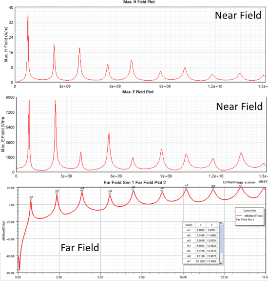
First and foremost, we can see, as expected, that both near and far Field have resonances at the same frequencies. Additionally, we can observe from Figure 1 that both E and H fields for near field have the largest radiation spikes at 786.3 MHz and 2.349GHz resonant frequencies.

Figure 1. Plotted E and H fields for both Near and Far Field solutions
If we plot E and H fields for Near Field, we can see at which physical locations we have the maximum radiation.

Figure 2. Plotted E and H fields for Near field simulations
As expected, we see the maximum radiation occurring over the air gap, where there is no return path for the current. Since we know that current is directly related to electromagnetic fields, we can also compute AC current to better understand the flow of the current over the air gap.
Compute AC Currents (PSI)
This feature has a very simple setup interface. The user only needs to make sure that the excitation sources are read correctly and that the frequency range is properly indicated. A few minutes after setting up the simulation, we get frequency dependent results for current. We can review the current flow at any simulated frequency point or view the current flow dynamically by animating the plot.

Figure 3. Computed AC currents
As seen in Figure 3, we observe the current being transferred from the energy source, along the transmission line to the open end of the trace. On the ground layer, we see the return current directed back to the source. However at the location of the air gap there is no metal for the return current to flow, therefore, we can see the unwanted concentration of energy along the plane edges. This energy may cause electromagnetic radiation and potential problems with emission.
If we have a very complicated multi-layer board design, it won’t be easy to simulate current flow on near and far fields for the whole board. It is possible, but the engineer will have to have either extra computing time or extra computing power. To address this issue, SIwave has a feature called EMI Scanner, which helps identify problematic areas on the board without running full simulations.
EMI Scanner
ANSYS EMI Scanner, which is based on geometric rule checks, identifies design issues that might result in electromagnetic interference problems during operation. So, I ran the EMI Scanner to quickly identify areas on the board which may create unwanted EMI effects. It is recommended for engineers, after finding all potentially problematic areas on the board using EMI Scanner, to run more detailed analyses on those areas using other SIwave features or HFSS.
Currently the EMI Scanner contains 17 rules, which are categorized as ‘Signal Reference’, ‘Wiring/Crosstalk’, ‘Decoupling’ and ‘Placement’. For this project, I focused on the ‘Signal Reference’ rules group, to find violations for ‘Net Crossing Split’ and ‘Net Near Edge of Reference’. I will discuss other EMI Scanner rules in more detail in a future blog (so be sure to check back for updates).

Figure 4. Selected rules in EMI Scanner (left) and predicted violations in the project (right)
As expected, the EMI Scanner properly identified 3 violations as highlighted in Figure 4. You can either review or export the report, or we can analyze violations with iQ-Harmony. With this feature, besides generating a user-friendly report with graphical explanations, we are also able to run ‘What-if’ scenarios to see possible results of the geometrical optimization.

Figure 5. Generated report in iQ-Harmony with ‘What-If’ scenario
Based on these results of quick EMI Scanner, the engineer would need to either redesign the board right away or to run more analysis using a more accurate approach.
Conclusion
In this blog, we were able to successfully run simulations using ANSYS SIwave solution to understand the effect of not following Dr.Bogatin’s advice on routing the signal trace over the gap on a 2-Layer board. We also were able to use 4 different features in SIwave, each of which delivered the correct, expected results.
Overall, it is not easy to think about all possible SI/PI/EMI issues while developing a complex board. In these modern times, engineers don’t need to manufacture a physical board to evaluate EMI problems. A lot of developmental steps can now be performed during simulations, and ANSYS SIwave tool in conjunction with HFSS Solver can help to deliver the right design on the first try.
If you would like more information or have any questions please reach out to us at info@padtinc.com.