I am writing this post after visiting the 27th SFF Symposium, a 3-day Additive Manufacturing (AM) conference held annually at the University of Texas at Austin. The SFF Symposium stands apart from other 3D printing conferences held in the US (such as AMUG, RAPID and Inside3D) in the fact that about 90% of the attendees and presenters are from academia. This year had 339 talks in 8 concurrent tracks and 54 posters, with an estimated 470 attendees from 20 countries – an overall 50% increase over the past year.
As one would expect from a predominantly academic conference, the talks were deeper in their content and tracks were more specialized. The track I presented in (Lattice Structures) had a total of 15 talks – 300 minutes of lattice talk, which pretty much made the conference for me!
In this post, I wish to summarize the research landscape in AM cellular solids at a high level: this classification dawned on me as I was listening to the talks over two days and taking in all the different work going on across several universities. My attempt in this post is to wrap my arms around the big picture and show how all these elements are needed to make cellular solids a routine design feature in production AM parts.
Classification of Cellular Solids
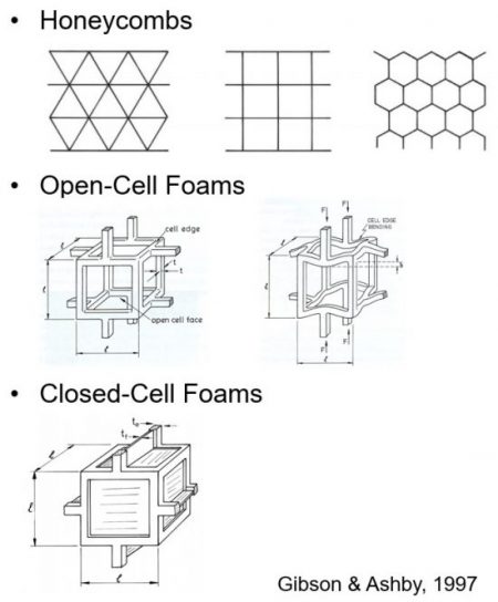
First, I feel the need to clarify a technicality that bothered me a wee bit at the conference: I prefer the term “cellular solids” to “lattices” since it is more inclusive of honeycomb and all foam-like structures, following Gibson and Ashby’s 1997 seminal text of the same name. Lattices are generally associated with “open-cell foam” type structures only – but there is a lot of room for honeycomb structures and close-cell foams, each having different advantages and behaviors, which get excluded when we use the term “lattice”.

The AM Cellular Solids Research Landscape
The 15 papers at the symposium, and indeed all my prior literature reviews and conference visits, suggested to me that all of the work in this space falls into one or more of four categories shown in Figure 2. For each of the four categories (design, analysis, manufacturing & implementation), I have listed below the current list of capabilities (not comprehensive), many of which were discussed in the talks at SFF. Further down I list the current challenges from my point of view, based on what I have learned studying this area over the past year.

Over the coming weeks I plan to publish a post with more detail on each of the four areas above, summarizing the commercial and academic research that is ongoing (to the best of my knowledge) in each area. For now, I provide below a brief elaboration of each area and highlight some important research questions.
1. Representation (Design)
This deals with how we incorporate cellular structures into our designs for all downstream activities. This involves two aspects: the selection of the specific cellular design (honeycomb or octet truss, for example) and its implementation in the CAD framework. For the former, a key question is: what is the optimum unit cell to select relative to performance requirements, manufacturability and other constraints? The second set of challenges arises from the CAD implementation: how does one allow for rapid iteration with minimal computational expense, how do cellular structures cover the space and merge with the external skin geometry seamlessly?
2. Optimization (Analysis)
Having tools to incorporate cellular designs is not enough – the next question is how to arrange these structures for optimum performance relative to specified requirements? The two most significant challenges in this area are performing the analysis at reasonable computational expense and the development of material models that accurately represent behavior at the cellular structure level, which may be significantly different from the bulk.
3. Realization (Manufacturing)
Manufacturing cellular structures is non-trivial, primarily due to the small size of the connecting members (struts, walls). The dimensions required are often in the order of a few hundred microns and lower, which tends to push the capabilities of the AM equipment under consideration. Additionally, in most cases, the cellular structure needs to be self-supporting and specifically for powder bed fusion, must allow for removal of trapped powder after completion of the build. One way to address this is to develop a map that identifies acceptable sizes of both the connecting members and the pores they enclose. For this, we need robust ways of monitoring quality of AM cellular solids by using in-situ and Non-Destructive techniques to guard against voids and other defects.
4. Application (Implementation)
Cellular solids have a range of potential applications. The well established ones include increasing stiffness-to-weight ratios, energy absorption and thermal performance. More recent applications include improving bone integration for implants and modulating stiffness to match biological distributions of material (biomimicry), as well as a host of ideas involving meta-materials. The key questions here include how do we ensure long term reliability of cellular structures in their use condition? How do we accurately identify and validate these conditions? How do we monitor quality in the field? And how do we ensure the entire life cycle of the product is cost-effective?
So What?
I wrote this post for two reasons: I love to classify information and couldn’t help myself after 5 hours of hearing and thinking about this area. But secondly, I hope it helps give all of us working in this space context to engage and communicate more seamlessly and see how our own work fits in the bigger picture.
A lot of us have a singular passion for the overlapping zone of AM and cellular solids and I can imagine in a few years we may well have a conference, an online journal or a forum of some sort just dedicated to this field – in fact, I’d love to assess interest in such an effort or an equivalent collaborative exercise. If this idea resonates with you, please connect with me on LinkedIn and drop me a note, or send us an email (info@padtinc.com) and cite this blog post so it finds its way to me.