ANSYS Electronics Desktop (AEDT) is a collection of powerful tools for simulation. AEDT Circuit provides time domain as well as frequency domain analyses. AEDT Circuit has high execution speed and robust ability to handle circuits of active and passive elements. Analysis types range from DC, Linear Networks (frequency domain), Transient, Oscillator, TV Noise, Envelope, Harmonic Balance, VerifEye (Statistical Eye Diagram), AMI Analysis, and more, with integrated support for additional co-simulation with tools like HSPICE or Matlab.
AEDT Circuit also provides an easy way to create and simulate planar structures such as microstrip, stripline, coupled lines, co-planar strips, co-planar waveguides, and other Printed Circuit Board (PCB) elements which can then be converted into a physical layout of the PCB. In this blog a simple workflow is explained to generate and model a planar structure in Circuit, then export the circuit model to HFSS 3D layout and HFSS for further analysis.
Define your substrate:
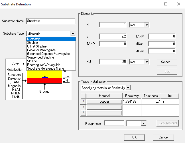
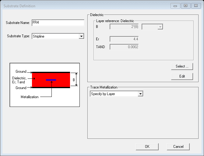
After inserting a Circuit Design, right-click on Data under project tree, choose Add Substrate Definition. This brings you to Substrate Defintion window that gives you many optios of substate types. You can choose the type of substarte you need and enter the dielectric and trace metalization information as shown in Figure 1. This substrate is used in calucalation of line impedances.
(a)
(b)
Figure 1. (a) Substrate Definition options of substrate types, (b) the definition of strapline used in this blog.
Define your stackup:
The stackup in Circuit is very similar to the stackup in HFSS 3D Layout. Please note that the definition of substrate is not automatically transferred to the stackup. The stackup needs to be defined by the user. Select the Schematic tab and from the top banner choose Stackup. Then define each layer. This stackup will be used in creating the layout and transferring it to HFSS 3D Layout. Figure 2 shows the stackup used for the FR4 substrate that was defined in Figure 1(b).
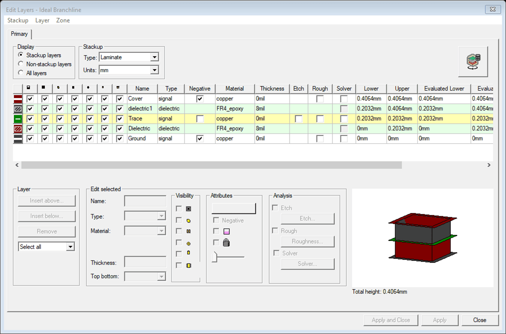
Figure 2. Stackup definition that will be used to transfer the layout to HFSS 3D Layout.
Create the circuit:
Circuit provides a large selection of component libraries. To see the Component Libraries, click on View and check Component Libraries. In the Component Libraries window look for Distributed and expand it. Under this category you see different types of PCB structures. We will use Stripline library. Expanding Stripline library there are various categories, including Transmission Lines. We need Transmission Line Physical Length component, as we would like to use pieces of transmission line to create an ideal branch line coupler. You notice by hovering the cursor on the name of the component a small information windows shows the symbol and information about the component, alternatively you can right-click on the name of the component and choose “View Component Help” to get to the complete help page about the component. Once a component is selected and placed in the circuit it will also appear under the Project Components list at the bottom of the Component Libraries list. This provides a quick way to reuse them (Figure 3).
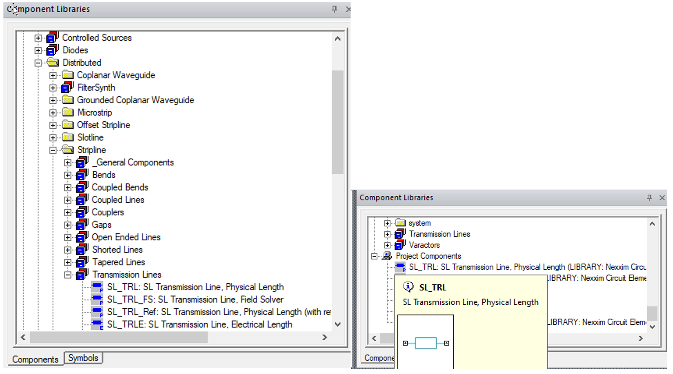
Figure 3. (a) Component Libraries, (b) Project Components and information window.
Let’s choose a physical length transmission line and place it on the schematic window. By double clicking on the symbol the Properties window opens and can be modified. Explicit values or parameters can be used to define the line properties.
Are you starting to calculate the line impedance to figure out the dimensions? Wait, there is a tool here that helps you do that. Click on TRL to open the line calculator. The line can be synthesized based on its impedance and electrical size by choosing the correct frequency and clicking on Synthesize (Figure 4). Using physical length transmission lines (50 and 35 ohms) and Tee lines and 4 ports I created an ideal branch line coupler (Figure 5). I ran a frequency analysis to make sure the circuit is working properly.
Before moving on to export the layout to HFSS 3D layout we can do one more step. To keep the substrate definition and reuse it layer, click on File->Save As Technology File. This would save the definition of stripline substrate in the personal library. Next step is to export the layout to HFSS 3D layout.
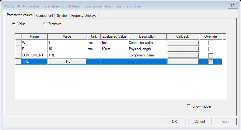
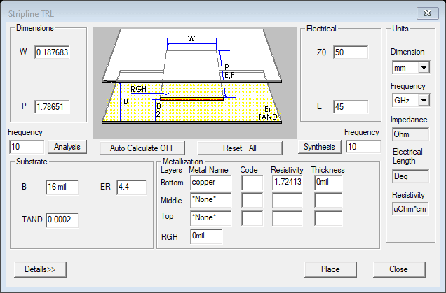
Figure 4. Properties and TRL windows.
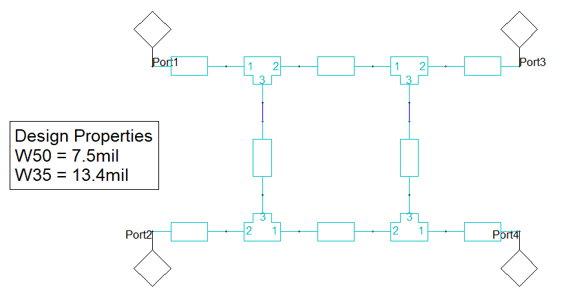
Figure 5. Branch line coupler schematic.
Export to HFSS 3D Layout:
Under Schematic tab, click on Layout, or from the top menu choose Circuit->Layout Editor. Notice that this layout editor is very similar to the HFSS 3D Layout window. Click Ctrl+A, to select everything. Then choose Draw form the top banner and click on Align MW Ports (Figure 6), notice that other tools are also available under Draw, such as Sanitize Layout and Geometry Healing. You might need to do a bit more corrections and cleaning before exporting the layout. Before exporting the geometry, you can also check the HFSS Airbox using Layout->Draw HFSS Airbox.
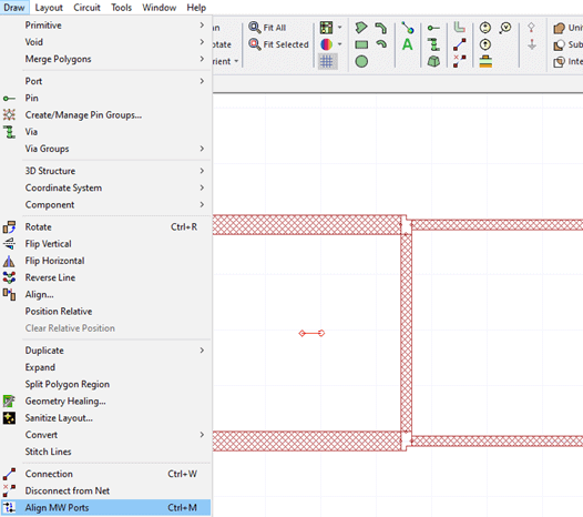
Figure 6. Aligning ports.
You may change the orientation to Isometric for a better view of the box (Figure 7).
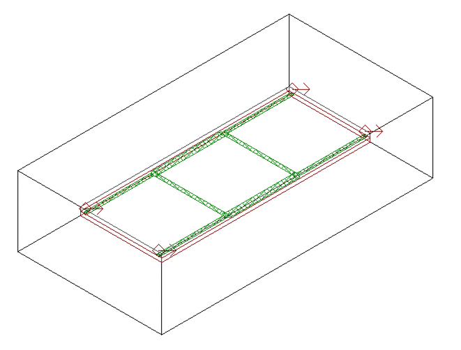
Figure 7. Layout editor in Isometric orientation, showing the HFSS airbox.
Make sure everything is still selected or select them with Ctrl+A, then under Edit, choose Copy to HFSS 3D Layout. Now an HFSS 3D Layout design is created. Open the design. There might be a few things you like to change. Expand the ports, the name of the ports might have changed. You also note that the ports are of Gap type. You can select the port and in the Properties window, under HFSS click on Gap and choose the Wave port. Just note that the wave port cannot be internal to the design. You might need to adjust the air box size or create PEC port caps in HFSS later.
The second point to consider is about the parameters defined in Circuit. Remember that we defined W35 and W50 as the line widths in Circuit. The parameter are transferred but several local variables are also created based on them. For example click on the 50 ohm line. The width is now shown as a new parameter. You can see the complete list of parameters that are created by choosing HFSS 3D Layout->Design Parameters. Under the Parameters Default you still see W35 and W50, but moving to Local Variables tab you see the parameters created based on the Parameters Default.
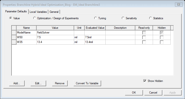
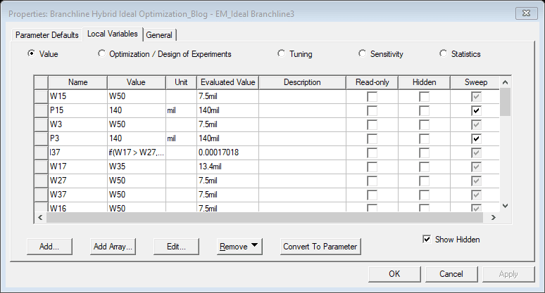
Figure 8. Properties window.
Export to HFSS:
Any HFSS 3D Layout design can be exported to HFSS. Click on Analysis from the project three. Right-click and Add HFSS Solution Setup (Figure 9). There is no need to run this analysis. It just needs to be created. Right-click on the HFSS Setup that was just created, select Export->HFSS Model (Figure 10). Select the name and location for this file. Open this file and examine the model. Notice that the parameters are not transferred to HFSS model, this is because all parts of the model are imported (Figure 11). The default ports (Gap ports) appear as lumped port. If you changed the Gap ports to Wave ports in HFSS 3D Layout, it is now the time to add the PEC port caps or change the airbox to make sure ports are not internal to the model.
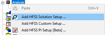
Figure 9. Adding HFSS solution setup.

Figure 10. Exporting the layout to an HFSS model.
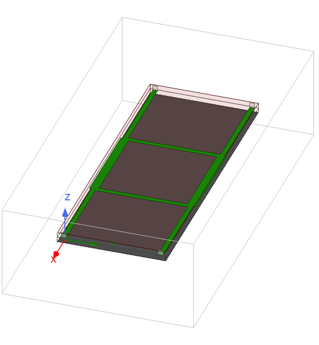
Figure 11. HFSS model.
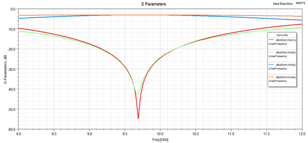
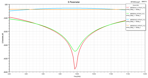
It is important to note that the type of analysis in Circuit is different than HFSS which will lead to slightly different result (Figure 12), which is expected and emphasizes the value of simulating structures in a full-wave field simulator like HFSS.
(a)
(b)
Figure 12. (a) Branch-line coupler S parameters from Circuit model, (b) the imported HFSS branch-line coupler S parameters.
Conclusion
This was a short blog showing the workflow for importing PCB and planar designs from AEDT Circuit to HFSS 3D Layout and HFSS. The workflow is a good method to quickly create the HFSS model of a planar structure.
If you would like more information related to this topic or have any questions, please reach out to us at info@padtinc.com.


